Repair and restoration of retro consoles, 8 bit computers. In this blog I hope to show you how to repair, retrore and modify old consoles and handhelds, from manufacturers such as Atari Amstrad Acorn Sinclair Commodore Dragon Sony MSX BBC Playstation Sega Microsoft xbox Spectrum ZX81 Vic 20 VIC20 C64 Amiga Binatone Grandstand.
Apologies for the delay with this entry; varied reasons include school holidays, two birthdays and some minor repairs of some retro console birthday gifts! Please feel free to use my PCB and 3D printed housing designs found on my Github and Thingiverse should you wish to make your own joystick adapter. Here is the TI994a working with the FlashRom99 and my Joystick Adapter circuit. Here are all the components required for this mod. The gerber files for my PCB design can be found on my Github. https://github.com/Alleged-Geek/TI99-4a-Joystick-Adapter/ And you are looking for the zip file named below if you are going to send the gerber file off to be manufactured. ti99-4a-adapter_2022-07-27.zip My github also contains stl files for printing the housing. And here is my version of the schematic diagram. You will need 10 X IN4148 signal diodes which can be found on eBay. 1 X DB9 D-SUB 9 Pin Female connector, again found on eBay. 2 X DB9 D-SUB 9 Pin Male connector al...
Get link
Facebook
X
Pinterest
Email
Other Apps
Commodore C16 Internal 64k RAM upgrade
Internal 64k RAM upgrade with hidden wires, testing
with the Diagnostics ROM and loading a 64K game using a Tapuino.
Many thanks to all who have posted about this mod on
the Internet… too many to list here.
In this one I have added my twist of geekery to it by
hiding the two external wires under the PCB.
Tools Required:
Soldering Iron
De-Soldering Tool (or Gun)
Cutters
Pliers
Screwdriver
Solder Wick (optional)
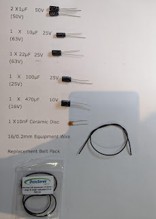
Parts Required:
2 X D41464C-10 DRAM IC’s
(I paid about £4:50 from eBay for
the pair including delivery)
2 X 74LS257 Multiplexer IC’s
(I paid £4:70 for the pair
from eBay)
2 X 16 Pin (turned pin) IC sockets
2 X 18 Pin (turned pin) IC sockets
Approx 1M of 30AWG Kynar wire
Solder
Firstly, strip down the C16.
Once stripped down to the PCB, look for the components
which will be replaced.
U5 and U6 are the TMS4416-15NL 16k DRAM chips.
And
U7 and U8 are the 74LS257APC Multiplexer Chips.
Below is a picture of their locations on the component
side of the PCB.
And
below is a picture of the locations of the vias to be de-soldered.
To help with the de-soldering process, it is a good
idea to add fresh solder to all the highlighted vias.
Below are a couple of methods of how to de-solder. The first
picture shows me de-soldering using my trusty de-soldering tool.
Basically, melt the solder with your soldering iron,
push the plunger down on the de-soldering tool the push the vacuum button to
suck the molten solder up into the solder sucker.
You may have to repeat this process on the component
side as the vias are plated through hole which means that the solder flows
through the PCB from the solder side to the component side.
If you are lucky enough to have a de-soldering gun then
this should make the de-soldering process a whole lot easier.
I am still getting used to my de-soldering gun and the
nozzle I used was too large which made de-soldering a wee bit more awkward.
Once most of the solder has been removed, test each pin
to see if it is free of solder before attempting to remove the IC.
Unfortunately, I had a camera malfunction whilst
de-soldering the IC’s so don’t have too many pictures of the process but if you
have a look at my earlier post (Umbrella fix for the ZX Spectrum +2) you will
see that I go into the de-soldering process in more detail.
If there is some solder left in the via, you could try
heating the pin of the IC with your soldering iron and gently moving the leg
until it is free.
This process took me over an hour using both techniques
explained above; I also used a flux pen and solder wick to assist the process
on stubborn joints.
Once removed you should have a PCB looking like this.
As you can see, they look pretty messy so it is a good
idea to clean up the area with some IPA and a cotton bud.
Once cleaned, visually inspect the vias for any damage
or excess solder in the vias.
Hopefully you will find that no damage has been done
whilst removing the IC’s.
Now we come to soldering in the IC sockets; I decided
to try something different for this mod. I wanted to try and keep the C16
looking like it’s original state so I decided that I would try and hide the two
wires taken from Pin 2 on U7 and Pin 14 on U8 underneath the PCB.
Both wires go to different points on the PCB which I
will show later.
My idea about how to do this was to use some thin wire
(30AWG Kynar wire) and hope that it would fit through the Vias of Pin 2 of U7
and Pin 14 of U8. So I tested my theory out and luckily for me, it was a
perfect fit!
So now I needed to modify the IC sockets for U7 and U8.
As usual, I prefer to use turned pin IC sockets so I
simply melted out the pin 2 socket of one 16 pin socket.
Then did the same for Pin 14 of the other 16 pin IC
socket.
After that, you should have sockets looking like this.
Now we need to prepare the 74LS257 IC’s for the Kynar
wire.
First of all, I cut short Pin 2 of the 74LS257 IC for
U7.
Add solder to the shortened Pin 2 of the replacement U7.
Then cut about 500mm of 30AWG Kynar wire.
Then strip and tin the end of that wire.
Finally solder the Kynar wire on to the shortened pin 2
of U7 ensuring that no un-insulated wire is showing below the shortened pin.
Then I repeated the process for Pin 14 of the 74LS257
IC for U8.
Now we can solder the IC sockets on to the PCB. Below
is a picture of their locations; the white silkscreen printing shows the
correct orientation of the IC sockets.
The first IC socket I soldered was the one for U7; this
one has the missing pin socket for pin 2.
Fit the IC socket and solder two opposite corner pins.
Once soldered in place check that the IC socket is sitting flat against the
PCB. If not simply heat up the solder on the raised pin and gently push the
socket flat against the PCB.
When soldering the socket for U7, remember not to add
solder to pin 2.
Fit and solder both the 18 pin IC sockets for U5 and U6
again ensuring that they are sitting flat against the PCB.
Now Solder the socket for U8 remembering not to add
solder to the via for pin 14.
I fitted the 74LS257 for U8 first; Feed the Kynar wire
through the space in the IC socket for Pin 14 and through the via on the PCB
for pin 14.
Then fit the 74LS257 IC into the IC socket.
Repeat the process for U7; feed the Kynar wire from pin
2 of the IC through the space in the IC socket and again through the via for
Pin 2 on the PCB.
Next fit the 74LS257 IC into the socket for U7.
Once done, you should have something looking like this.
Now we need to solder the Kynar wires on to certain
points on the PCB. Below is the location for the wire coming from pin 2 of U7.
Route the Kynar wire from pin 2 to the solder point on
the PCB. I used blue tack to hold the wire in place whilst I did this.
Then cut the Kynar wire to length.
After that, strip a small amount of insulation off the
end of the Kynar wire and tin the end of the wire to assist with the soldering.
Then add solder to the highlighted solder point shown
above.
Finally solder the Kynar wire on to the solder point on
the PCB.
Repeat the process for the wire coming from Pin 14 of
U8.
Below is the location of the solder point.
Route the Kynar wire and trim to length.
Strip and tin the end of the Kynar wire.
Add solder to the solder point then solder the Kynar
wire into position.
I decided to check the wiring with my multimeter;
checking for short circuits between pin 2 of the modified U7 IC and pin 2 on
the via at pin 2 of U7. This was open circuit which is exactly what I was
looking for.
I did the same for Pin 14 of the modified U8 IC and the
via for pin 14 of U8; again this proved to be open circuit.
I then checked that the wires were soldered to the correct
points on the PCB.
Everything was looking good so I fitted the replacement
D41464C-10 DRAM IC’s U5 and U6.
Reassemble the C16.
Then set up the C16 and test.
Nervous times!
Yay! A successful test! Reading 60671 Bytes Free.
Looking good so far.
But I know how temperamental DRAM can be so I decided
to test the RAM using my Diagnostics ROM.
Remove the Kernal ROM.
Then fit the Diagnostics ROM.
Reassemble the C16 and fit the loopback connectors for
the Serial and Cassette Ports.
Then test!
Again nervous times!
Another success; I was treated to the woo-hoo at the
end of the Diagnostics test!
Now it was time to try out the memory upgrade properly;
this time I was going to load a game designed for the Plus 4.
The first thing I had to do was to replace the
diagnostics ROM with the Kernal ROM.
Then hook up the C16 to the TV again.
Then using my Tapuino, I attempted to load Mercenary –
Escape from Targ.
Looks good so far…
Still loading…
Load successful!
We have a fully functioning 64K C16 computer!
Below is a clip of this process from start to finish.
Thank you for taking the time to read this entry; I
hope you have found it useful.
If you have any questions or queries about this mod
then please feel free to leave a comment or email me directly at


Comments
Post a Comment