Repair and restoration of retro consoles, 8 bit computers. In this blog I hope to show you how to repair, retrore and modify old consoles and handhelds, from manufacturers such as Atari Amstrad Acorn Sinclair Commodore Dragon Sony MSX BBC Playstation Sega Microsoft xbox Spectrum ZX81 Vic 20 VIC20 C64 Amiga Binatone Grandstand.
Apologies for the delay with this entry; varied reasons include school holidays, two birthdays and some minor repairs of some retro console birthday gifts! Please feel free to use my PCB and 3D printed housing designs found on my Github and Thingiverse should you wish to make your own joystick adapter. Here is the TI994a working with the FlashRom99 and my Joystick Adapter circuit. Here are all the components required for this mod. The gerber files for my PCB design can be found on my Github. https://github.com/Alleged-Geek/TI99-4a-Joystick-Adapter/ And you are looking for the zip file named below if you are going to send the gerber file off to be manufactured. ti99-4a-adapter_2022-07-27.zip My github also contains stl files for printing the housing. And here is my version of the schematic diagram. You will need 10 X IN4148 signal diodes which can be found on eBay. 1 X DB9 D-SUB 9 Pin Female connector, again found on eBay. 2 X DB9 D-SUB 9 Pin Male connector al...
Carrying on with the modification of my £5 ZX Spectrum
+2 I decided to do what is known as the ‘Umbrella’ fix. On the ZX Spectrum 128
Toastrack and the +2 there is a known glitch where there is a raining effect on
the graphics of certain games during gameplay.
You can see the problem on the picture below where
there are loads of horizontal lines running across the screen.
Luckily there is a fix for this thanks to a clever
piece of programming from Velesoft. Information and the download link for the
code can be found on the link below.
An Eprom Programmer, my one
is a TL866 II Plus shown below (I think I paid about £40 for my one about a
year ago but they appear to have gone up in price a wee bit since then)
You will also need a GAL16V8D which can be picked up on
eBay from as little as £2 each.
It would be worth ordering a 20 Pin 0.3” pitch IC
Socket at the same time as this will make removal of the IC afterwards a whole
lot easier. I recommend using a turned pin socket for this as that will make it
easier to repair any trace damage done to the component side of your +2’s PCB
whilst removing the original HAL IC
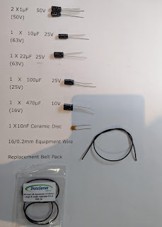
Finally you will need a small piece of wire to connect
pin 11 of the new GAL IC to pin 28 of the Z80 CPU. For this I used some of my Kynar
wire (or wire wrap wire as I know it… again showing my age!) but any old wire
will do (within reason)
If you don’t want the expense of buying an eprom
programmer, you easily find a pre-programmed GAL16V8D chip online for around £5
Now we have the parts, lets get started!
Firstly I am going to programme the GAL16V8D IC.
Download the zip file containing the new code for the
GAL chip; the link below is a direct download for the ZIP file
Now double click on the
XGpro icon to start the programmer software.
Then click on the Select IC box located at the top left
of the software window
Then type GAL16V8D in the field as shown below
There should only really be one manufacturer (LATTICE)
and the Device we are looking to programme is the one simply called GAL16V8D.
To find out the correct orientation of the IC in the
programmers ZIF socket click READ.
A pop up window will then show you where and how to
place the GAL chip into the programmers ZIF socket.
As you can see from the picture above, pin 1 of the IC
is located closest to the ZIF socket lever. Place the GAL IC into the
programmer as shown below.
Then click READ on the software.
If the IC is blank, all the data in the data field
should read 1’s as shown below.
Don’t worry if your IC is not blank as the IC as unlike
the write once ROM’s I used for the ZX Diagnostics project, the GAL chip can be
erased and rewritten as often as you like by simply clicking on the Erase icon
within the software.
Now click LOAD.
And then load the galnew.jed file we downloaded
earlier.
You should see that the data in the field now has a
series of 1’s and 0’s
I scrolled through the data to check that everything
was in order then clicked PROG.
When the programmer pop up windows appears, it is
important that you uncheck (de-select) the LOCK Bit option
Now Click Program.
And hopefully you will get the same message as shown
below.
Now click BACK and have a quick look at the data in the
data field.
Now it is time to double check that the IC has been
written correctly.
Click READ, then click Read in the pop up window.
Now click BACK to view the data
If you forgot to uncheck the LOCK Bit option, the data
will not be correct and it will look different to the image shown below. If
this is the case, simply erase the IC and restart the programming process from
the beginning.
If the data on the GAL chip looks similar to that
above, exit the software… Well done, you have successfully written your
GAL16V8D IC with the Umbrella fix software!
Now let’s turn our attention to the ZX Spectrum +2
Disassemble the +2 and have a look for the HAL10H8 IC
(IC7 on the Issue 3 PCB) I have highlighted it in the picture below.
Note that all the IC’s have their notches facing south
as we look at the PCB.
Below is a close up of the HAL chip.
Now let’s have a look at the solder points on the
solder side of the Issue 3 PCB.
Below is a picture of the location of the pins in
question as well as a close up shot of the pins we need to de-solder.
Time to get my trusty de-soldering tool out again but
before we do so, it is a good idea to freshen up the solder on the IC as this
should make de-soldering a whole lot easier.
Now de-solder all 20 pins of the IC; take care doing
this as it is very easy to damage the traces on the 35 year old computer.
Inspect
the de-soldering job then gently nudge the legs of the IC with something like a
spudger to see if they are free.
If there are some legs still soldered you can try to
reapply solder then de-solder again.
After that if there are some legs still soldered, you
can try and gently nudge the legs to the middle of the via with your soldering
iron.
Inspect again (you really don’t want to damage the PCB)
and if everything looks free try and gently pry the IC up from the component
side. I used my plastic pointy spudger to do this as I did not want to damage
the board with a screwdriver.
Disaster! I felt resistance and a cracking sound...
Something wasn’t right!
Let’s have a look at pin 5 of the IC leg.
If you look closely you will see what appears to be a
blob of solder on pin 5 of the IC. This usually means that a trace or plated
through hole via has been removed when lifting the IC from the circuit board! I
was beyond the point of no return now so I gently lifted the remaining legs of
the IC out of the circuit board. Now I would have to deal with any damage done
to the traces. So it was out with the magnifier glass to closely inspect the
PCB.
Upon inspection of the component side I lucked out as
there were no traces leading to and from pin 5 of the IC! Now the part I was
dreading… the solder side! Time to get that magnifying glass out again.
YES! No damage done to the solder side of the PCB… I
got lucky! A simple rookie mistake could have ended up with lifted traces. I
should have triple checked before trying to lift the IC!
Time to clean up the de-soldered area, for this I used
IPA and a cotton bud.
Time to inspect the area again, this time I was looking
for solder shards from the de-soldering process as well as any short or open
circuits.
All looks good, now time to solder in the IC socket.
For this I would always recommend turned pin IC sockets as it is easier to
solder wires on to the pins from the component side should there be any damage.
The cheaper IC sockets cover the vias completely making it difficult to repair
any damage on the component side.
Solder the IC socket on to the PCB; ensure that the
notches match the IC and silkscreen print.
We really want the IC socket to be seated correctly and
flat against the PCB so a wee trick is to solder the opposite corner pins of
the socket then reflow the solder on any raised side whilst pushing gently down
on the socket until the socket is fully flat against the surface of the
component side.
The reason we do this is because we will be pushing the
replacement IC down on to the socket; if it is raised at all there is a
possibility that when you push the IC down you can also push the socket pins
down which can lift the traces on the solder side.
Solder the opposite corners then check that the IC is
seated correctly.
Once happy solder the remaining pins of the IC then
inspect the soldering, looking for any short circuits or poor solder joints.
You are also looking to see if the solder has flowed
through the plated through vias from the solder side to the component side
(this will also confirm that no other damage was done to the through hole
traces when de-soldering the HAL chip)
With the IC socket in place it is time to hard wire pin
11 of the GAL16V8D IC (RFSH) to pin 28 of the Z80 CPU (RFSH).
I used my Kynar wire for this but any wire would do
within reason (although a heavier gauge will be awkward to solder).
First up, solder one end of the wire to pin 11 of the
GAL chip.
Try and minimise the amount of bare wire on the wire
when soldering. I like to have it so that the insulated part of the wire almost
touches the pin being soldered on to. I also try to ensure that no bare wire is
showing on the other side of the pin being soldered on to. This will help avoid
any short circuits.
Tin the ends of your wires before soldering them on to
the pins (add solder to the bare wire)
Then route the wire to Pin 28 of the Z80, carefully cut
the wire to length without damaging your circuit board, tin the end of the wire
then add fresh solder to pin 28 of the Z80 (which will make soldering the wire
to the pin a whole lot easier) after all that, solder the wire to pin 28.
And this is what it should look like.
After soldering the wire it is always a good idea to
check your wiring with a multimeter (either in ohms or continuity modes).
I turned the PCB over so that I could do this test on
the component side and connected one probe to pin 11 of the IC socket for the
GAL chip then the other to pin 28 of the Z80.
Now fit the GAL16V8D IC to the PCB
Before we fit the IC we will need to straighten the
legs; I used my leg straightening tool of which there are several varieties but
you could simply roll the legs straight on a flat surface if you don’t have a
straightener.
Now fit the IC paying close attention to the
orientation (all notches should face south in an issue 3 ZX Spectrum +2)
Below is a picture showing pin 1 of the GAL16V8D IC
And below is a picture showing where Pin 1 of the IC
socket on the PCB is.
Now fit the GAL chip then check to ensure that all the
pins have located into the socket correctly.
Now it is time to reassemble the +2
Secure the PCB using the six small self tapping screws.
Fit the voltage regulator.
Fit the keyboard membrane.
Fit the cassette PCB connector.
Finally screw in the six case screws.
Now it is time to test the +2… nervous times!
Plug everything in
There is a good picture; if the GAL16V8D chip is
faulty, coded incorrectly or not connected you will get a black and white
chequerboard screen.
Now load up a game which is affected by the umbrella fault;
in this case I loaded up Robocop 3 again.
Then wait…
…
…
And wait…
…
…
The 128k games take ages to load! This one took nearly
10 minutes! So glad I have the TZX Duino Amplifier fitted, I would have hated
to get a tape loading error ;)
Game finally loaded.
And look, no raining effect! Job Done! Even Leo was
impressed!
Youtube clip of the entire process is shown below
Well, I have had so much fun doing this repair; it is
always good to get to use tools or equipment which I don’t usually use such as
my Eprom programmer.
Many thanks to the clever folks at velesoft.speccy.cz
for making their modification public.
This repair was easy on paper but a lot of care should
be taken when removing the old HAL chip. It is very easy to damage the PCB
traces on your +2, my rookie mistake was not to check the soldering on the
component side correctly before removing the HAL chip. My only defence is that
I checked that all the pins were loose on the solder side and gave the
component side a quick look over before removing the IC.
Anyway, I hope that you found this entry useful; If you
have any questions or queries about this fix, please feel free to leave a
comment or email me directly at


Comments
Post a Comment