Repair and restoration of retro consoles, 8 bit computers. In this blog I hope to show you how to repair, retrore and modify old consoles and handhelds, from manufacturers such as Atari Amstrad Acorn Sinclair Commodore Dragon Sony MSX BBC Playstation Sega Microsoft xbox Spectrum ZX81 Vic 20 VIC20 C64 Amiga Binatone Grandstand.
Apologies for the delay with this entry; varied reasons include school holidays, two birthdays and some minor repairs of some retro console birthday gifts! Please feel free to use my PCB and 3D printed housing designs found on my Github and Thingiverse should you wish to make your own joystick adapter. Here is the TI994a working with the FlashRom99 and my Joystick Adapter circuit. Here are all the components required for this mod. The gerber files for my PCB design can be found on my Github. https://github.com/Alleged-Geek/TI99-4a-Joystick-Adapter/ And you are looking for the zip file named below if you are going to send the gerber file off to be manufactured. ti99-4a-adapter_2022-07-27.zip My github also contains stl files for printing the housing. And here is my version of the schematic diagram. You will need 10 X IN4148 signal diodes which can be found on eBay. 1 X DB9 D-SUB 9 Pin Female connector, again found on eBay. 2 X DB9 D-SUB 9 Pin Male connector al...
Get link
Facebook
X
Pinterest
Email
Other Apps
Fixing the Flickering Screen Problem I had when Using a SCART lead on the ZX Spectrum +2
This is part 2 of my restoration series of my £5 ZX
Spectrum +2. However this was an unexpected modification; I tried out my new
scart cable for the +2 after fitting and testing my TZX Duino amplifier. The
amp worked flawlessly but the picture quality wasn’t the best on my +2. Well,
the picture was ok in truth but I kept on getting a flickering of the screen
which was even worse during gameplay.
After a bit of reading, I found that my version of the
+2 had some transistors put in the wrong way round during manufacture. Surely
this was a good place to start? However after replacing them with new ones and
in the correct orientation, the picture quality got even worse!
I double checked my soldering and continuity between
components and everything was good so it was back to the internet for some
clues.
I stumbled across this page on spectrumforeveryone.com
and it looked simple enough; in fact, I think that the
flickering screen may have actually been cured by this mod had I done it first.
This entry will take you through the complete process
of replacing the transistors to doing the modification found on
Spectrumforeveryone.com
Now let’s get started!
Firstly I will show you some pictures of the original
flickering screen problem.
Whilst loading Monty on the Run I noticed this.
Below is an image of the stable picture before the
flicker.
And below is an image of the flicker
Then it returned to normal
The flicker only lasted about half a second but the +2
kept on doing it during the loading sequence and was even worse during gameplay
when there were actual moving pictures on the screen.
I had heard that there were some grey +2’s which had
TR4, TR5 and TR7 inserted in the wrong orientation during manufacture so I thought
that it would be a good place to start.
Below is a close up of the schematic
showing TR4.
As you can see from the image above, the emitter of the
2N3904 is connected to a 75 Ω resistor and the collector to +12V and the
positive of C6
Here is a pinout of the 2N3904
I decided to test this out with my multimeter
The multimeter buzzed meaning that the emitter was
indeed connected to the +ve of C6 (the wrong way round)
I tested TR5 next; here is a close up of the schematic
Here you can see that the emitter is connected to R57
and pin 5 of IC12, time to test with my multimeter.
I connected the probes to the collector of TR5 and to
R57 and pin 5 of IC12 and again the multimeter buzzed proving that this
transistor was in the wrong way round as well.
Finally,
I tested TR7 in which the emitter is connected to R64
The multimeter sounded meaning that the collector was
connected to R64 (the wrong way round)
Time to dig out my solder sucker!
Firstly let’s have a look at the position of TR4
on the component and solder sides of the PCB.
The above image shows that TR4 is located next to the
modulator on the component side of the PCB
And below I have highlighted the middle pin (Base) of
the 2n3904 on the solder side of the PCB
Time to desolder.
Before I attacked the transistor with my soldering iron
and solder sucker, I found that a couple of the legs of the transistor were
sticking up slightly after the solder joint.
In my experience, they can be hard to remove when like
this as the PCB is plated through hole (meaning the solder will fill the via
between layers of the PCB) If the solder cant be removed completely between
layers then it can be tricky to reflow the solder and gently pull the component
out therefore the shorter the length of leg to remove the better.
It will also make it easier to position the solder sucker
on to the via.
Time to get my cutters out.
Trim the excess legs of TR4
Then desolder; I tried using my new electric
desoldering tool for this job but found
that it just isn’t all that good so I reverted back to my trusty 20 year old
solder sucker!
Then place the new 2N3904 in the TR4 position in the
opposite orientation to the silkscreen printing (White component profile
printing on the PCB) Basically, the flat edge of the new transistor should be
placed where the curved line is shown on the PCB as shown below.
Once placed in the correct orientation, solder the
transistor as seen in the picture above.
Now let’s have a look for TR5.
Component side.
Solder side with the middle pin (Base) highlighted.
Time to desolder...
I ended up reverting to my ancient solder sucker as
again the electric desoldering tool didn’t really work for me.
Below is a picture of the removed transistor.
Fit then solder the new 2N3905 in the TR5 position,
again ensure that the flat face of the transistor is orientated on the curved
side of the image on the silkscreen.
Below is a picture of the refitted transistor.
Finally change TR7, below is a picture of its location
on the component side of the PCB
Now let’s find it on the solder side; highlighted is
the centre pin (Base) of the 2N3904.
As you can hopefully see, there are thin traces very
close to the via’s on either side. All the traces leading to other parts of the
circuit board are located on the component side.
Great care should be taken when removing this component
as it would be easy to break the traces on the solder side with an accidental
slip of the soldering iron.
Also, and if using the melt solder and gently pull the
component out from the component side technique it is very easy to lift the
traces from the component side.
To try and help me with the dsoldering process, I added
fresh solder to the original solder joints.
Then I attacked it with my solder sucker.
It still wouldn’t budge so I tried the heat (to melt
the solder) and gently pull the component out through the component side.
Eventually
it came out; the picture below shows the removed transistor.
Time to refit and solder a new 2N3904 in the TR7 position.
Ensure that it is placed the opposite way round than the silkscreen advises.
Now that the three video transistors have been replaced
in their correct orientation it is time to refit the +2 and test. Firstly
inspect the PCB for any solder shards left from the desoldering process. Then
when happy refit all the parts in the +2 and test the system.
Firstly, refit the main PCB to the bottom half of the
+2 using the six small screws.
Then refit the voltage regulator.
Carefully refit the two keyboard membrane ribbons
Then refit the cassette PCB connector
Refit the lid
Then refit the six case screws
Set the system up
My first impressions weren’t good; the screen looked
grainy and nowhere near as clean as it was before replacing the transistors.
But my troubles worsened, the following pictures show
what happened when I tried to load a game.
Basically
as well as being of a poorer quality signal, I was now experiencing loss of
signal!
Was it my soldering?
Did I damage the PCB when replacing the transistors? I did not know!
So I spent
the next hour checking and rechecking my soldering and traces on the PCB. I
also checked continuity between the relevant components. Everything came back
good! Time to do a wee bit more research on the internet!
Luckily, I
found a page entitled ‘making-your-12822a3-rgb-socket-scart-compliant’ on the
spectrumforeveryone website (link below)
below is a
screenshot of the page in question with the very simple instructions of how to
do the modification.
The
instructions say to remove LK4 then link LK2 and then replace the 1kΩ
resistor in the position R9 with a 680Ω resistor.
I guess, it
was time to open up the +2 again!
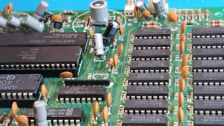
Firstly I
looked for L4
The above
photo shows LK4 on the component side (next to the RGB connector and modulator)
The picture
below shows the position of LK4 on the solder side of the PCB.
LK2 can be
found next to LK4
The above
image shows LK2 from the component side
The pictures
above show the solder side position of LK2
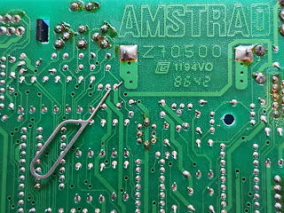
Desolder
LK2 and LK4
Now let’s
find the 1k Ω
resistor R9
This was
very strange! There wasn’t a resistor in the space for R9, another
manufacturing mistake? Or is this standard? I really don’t know!
I decided
to remove the solder in the position for R9 so that I could fit a 680Ω
resistor.
Firstly I needed to
identify which vias I needed to desolder.
Desolder
the vias
Now we can
fit a new link into position 2 as well as fit a 680Ω
resistor into R9
But…
I didn’t have
any 680Ω
resistors in stock!
And
I was in
the zone!
I wanted a
repair fix today…
Not in
however many days it would take to get a 680Ω resistor.
So
I
improvised!
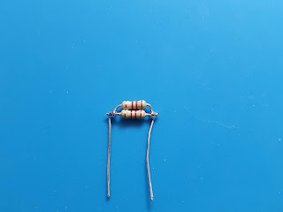
I did have some
1k2Ω
resistors, so I paralleled them up and tested with a meter, the actual value
came out at 604Ω. Hopefully the relatively small
difference in value wouldn’t cause me any issues.
Below are some pictures of
how I paralleled the two resistors to fit neatly into the circuit.
I used the
leg of one of the resistors to make a new wire link as the old one was a little
buckled and bent after the removal process. Note that I intentionally left one
leg longer than the other to make it easier to fit.
Now all I
had to do was solder them into the circuit.
Firstly I fitted
and soldered LK2.
Then I
filled the vias with solder at position LK4.
Next I
fitted and soldered my parallel resistor into the position R9
Now all I
had to do was to refit the +2, set up and test for the second time during this
mod.
Follow the
instructions for refitting and setting up the +2 as shown earlier in this entry then
test.
Nervous times
ahead!
I plugged
everything in and powered up the +2…
And…
…
…
Looking
good!
The grainy
picture was back to a nice clean crisp picture, now lets test it out loading a
game…
No sign of
the flickering video or loss of signal… I am impressed!
Even Leo ‘The
Terrible’ purred his approval!
Time to
play some Monty on the Run
Great game,
great picture… all let down by my rubbish gameplay!
Below is a
youtube clip of the whole process from start to finish.
Well, this mod
should have taken a couple of hours at most but ended up taking most of the day…
but… I am not complaining at all as I absolutely love fault finding and
researching solutions! This was geek heaven to me!
Upon
reflection, I think that I would have gotten away with simply doing the
modification I found on spectrumforeveryone.com but that wouldn’t have given me
the chance to repair the manufacturing error in the process.
This was a
great wee project and I am planning my next instalment for the +2 as I write
this.
Many thanks
again for taking the time to read through this entry; I sincerely hope it was
of some use to you.
If you have
any questions or queries, then please feel free to leave a comment or send me
an email to


Comments
Post a Comment