Search This Blog
Repair and restoration of retro consoles, 8 bit computers. In this blog I hope to show you how to repair, retrore and modify old consoles and handhelds, from manufacturers such as Atari Amstrad Acorn Sinclair Commodore Dragon Sony MSX BBC Playstation Sega Microsoft xbox Spectrum ZX81 Vic 20 VIC20 C64 Amiga Binatone Grandstand.
Featured
- Get link
- X
- Other Apps
Designing, building and fitting a TZX Duino Amplifier for the ZX Spectrum +2
Having fun with my £5 ZX Spectrum +2
Part 1
Designing, building and fitting my TZX Duino Amplifier
I have two working ZX Spectrum +2’s, the one I am going to have fun with is the one which I won for the outrageous price of £5 at auction in Aberdeen. The other I am going to keep as original; I tend to do this when I have two of the same computer or console. When I only have one computer or console I like to try and make my modifications fully reversible so that I can easily put them back to their original state should I wish in the future.
I have a lot of plans for this Spekky and I think that this will be a multiple entry blog post.
To start things off, I am going to modify the Spectrum so that I can use my own TZX Duino design to load software on the classic computer. As you may know, it is quite difficult to load software from an external device on to the Spectrum due to the fact that the internal data recorder is temperamental with the input levels. I have tried loading games from my phone using a tape to 3.5mm headphone jack but this doesn’t always work. So after a bit of research I stumbled across a familiar face (from the same person I found the ZX81 composite video mod schematic)
He has produced a massive seven part youtube series on the restoration of a poorly ZX Spectrum Plus 2.
In this case, the information I needed was on part three
https://www.youtube.com/watch?v=qUIv-A_DOc0&t=0s
During the video, JoulesperCoulomb goes into great detail about the modification and the development of the circuit.
Here is a screen grab of his schematic diagram
I took his design and recreated it using Eagle
I then designed the PCB; I had an idea about where I wanted to place the circuit so after a bit of measurement I came up with this design.
I then manufactured a prototype and after successfully testing it, I sent my design off to JLPCB for manufacture. Here are the pictures I managed to download from JLPCB when I uploaded my gerber files.
After a couple of weeks, the PCB’s turned up from China and as usual, they look fantastic!
Full details about this design can be found on my
Github.
Below is a parts list and ordering information from Rapidonline.com (it may be cheaper to buy from Ebay or Amazon because of the postage costs from Rapid but the order codes will show you the correct components needed for this PCB)
1 X 62-0414 TruOhm CR-025 68K Carbon Film Resistor 0.25W - Pack of 100 £0.86
1 X 62-0418 TruOhm CR-025 100K Carbon Film Resistor 0.25W - Pack of 100 £0.86
1 X 62-0434 TruOhm CR-025 470K Carbon Film Resistor 0.25W - Pack of 100 £0.86
20 X 47-3142 DC Components 1N4007 1A 1000V Silicon Rectifier Diode £0.80
5 X 22-1720 TruConnect 8 Pin 0.3in Turned Pin Socket £1.56
10 X 08-0307 0.022uF 5% 100V 5mm Pitch Faratronic Polyester Film Capacitor £0.84
5 X 11-0810 Forever 22uF 20% 10V 85°C 7mm Micro Miniature Radial Aluminium Electrolytic £0.27
5 X 21-1560 CamdenBoss CTB1500/2 2 Pole Commercial Standard Profile Screw Terminal 5mm £0.78
5 X 21-1575 CamdenBoss CTB1500/6 6 Pole Commercial Standard Profile Screw Terminal 5mm £1.69
5 X 82-0332 Texas Instruments LM358AP Low Power Dual OP Amp
£2.36
Total cost of parts for the manufacture of 5 PCB’s is £10.88
I base my costing for 5 PCB’s as this is the minimum order from most PCB manufacturers.
You will also note that the PCB connectors are a wee bit different to the ones I actually used as the ones I had in stock at home were a wee bit more expensive. The only real difference is that the ones listed in the parts list above are screw terminals and not push button ones. Also, I replaced the1N4004’s with a 1N4007 as they were also cheaper (any rectifier type diode will do)
Now let’s get soldering!
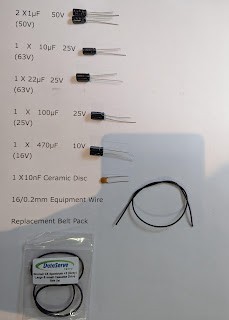
I laid out the components in order before soldering.
Starting with the lowest resister value up to the highest, then the diodes, IC Socket, polyester capacitors, electrolytic capacitor, PCB terminal blocks and finally fitting the IC.
It is good electronics practice to start with the lowest physical height component first then build up to the tallest one last. For example, if you started with the electrolytic capacitor first, the PCB would be unstable and wobble when soldering the remaining components. It is also easier to ensure that the components are sitting flat on the PCB.
Solder in the 68kΩ resistor in position R8
Next Solder R1 and R3 both 100kΩ into their correct position. Note that it is easier to solder in a couple of components at a time because if you load all the components on to the PCB, the legs sticking through the PCB will get in the way of the soldering iron.
Next up was R6 which is also a 100kΩ
Then Solder in R7 and R9 (also 100kΩ)
The last two 100kΩ resistors go in positions R2 and R4
Now solder the 470KΩ resistor into position R5
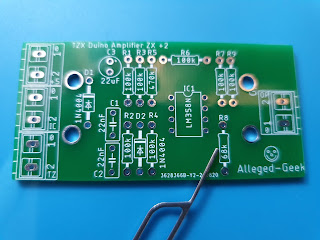
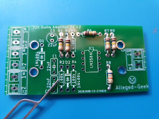
Next to be soldered are the two diodes D1 and D2. It is important that they are placed in the circuit the correct way round. The photo of the Diode below has the Cathode highlighted with the pin and below that I have highlighted the Cathode on the PCB with a pin.
Ensure that the cathode leg of D1 is placed in the highlighted position shown below and the anode in the Via below.
Then place the cathode of D2 in the position highlighted below and the anode in the other Via of D2.
Now solder in the IC socket (if you are using one) Ensure that the notch of the IC Socket matches the notch highlighted on the silkscreen print of the PCB.
Now try and ensure that the IC socket is soldered flat on the PCB. The best way to do this (so that you can easily fix) is to solder the two highlighted pins on the solder side of the PCB. If the socket is raised on any corner it is a simple job to heat and melt the solder on the raised side then push the socket up on that corner once the solder has melted.
Check that the socket is seated correctly; repair if not then solder the remaining six pins on the IC socket.
Now solder the two 22nF Polyester capacitors into positions C1 and C2 on the circuit board. It does not matter which way round they go but it is good practice to have the writing (values) facing the same way which makes reading the component values on the PCB a whole lot easier.
Now we have to solder in the 22uF Electrolytic capacitor. It is very important that this is soldered in the correct orientation as failure to do so will result in a damaged capacitor (it may even explode!)
Highlighted below is the negative leg of the capacitor. When new, most electrolytic capacitors have a shorter negative leg. If unsure, check that there is a light stripe on the body of the capacitor with a (-) sign printed on it by following the short leg of the capacitor up to the body of the capacitor.
Below is a highlighted picture of the negative leg of the 22uF capacitor.
Below is the position on the PCB for the negative leg of the capacitor.
There are only the connectors to solder in place now; the connectors I used with this PCB are a wee bit more expensive than the ones I suggest you use on the partslist. They are also a wee bit more awkward to fit as you have to join three two way connectors together to give a six way connector for the left hand side of the PCB.
The ones I recommend you use are cheaper and easier to fit as they are already a two way and a six way connector.
But I will show you how I fitted my connectors together anyway.
Join three connectors together as shown below.
The holes of the connectors should be facing outwards on the PCB. I have highlighted the holes on the single two way connector below.
Place the two way connector in the position shown and the six way connector on the other end of the PCB.
Then solder the two end pins of the six way connector. It is quite important that they are sitting flat against the PCB as if they are raised it could lead to a broken trace when you push down on the button when inserting the wire to the connector.
Melt the solder and push the connector as flat as you can on the PCB if there are any gaps showing.
This one was good so no adjustment was required.
Once flat, solder the remaining legs of the connector. Ensure that the two way connector is seated flat against the PCB as well.
Now fit the LM358 IC; straighten the legs either using a leg straightening tool or simply push the pins down on a flat surface to straighten the legs manually.
Examine the IC; some have a notch cut out of the plastic in the middle of the Pin 1 end, this one however has pin 1 highlighted with a small hole on the plastic beside pin 1.
Pin 1 of the IC should go in the highlighted via as sown in the picture below.
Once fitted you should have a PCB looking like this.
This next part is optional; if you have some IPA, clean the flux residue (left on the PCB during the soldering process) I use a spray and a toothbrush to clean any excess flux off the PCB.
Spray on the solder side of the PCB.
Clean with a toothbrush, and then buff up with a cotton bud.
And afterwards you should have a sparkling clean PCB as shown below.
And that is the population of the ZXDuino Amplifier PCB complete. Now all we have to do is fit it!
Now it is time to fit the amplifier into the Plus 2!
For the fitting of the amplifier you will need the following items
Either a mono or stereo 3.5mm chassis mount audio jack socket
Some heatshrink sleeving
300 mm of black and white 7/0.2mm equipment wire (or equivalent)
300mm black, red and yellow 7/0.2mm equipment wire
2 Aluminium cable clips (optional)
100mm cable ties
4 Adhesive PCB Stand offs
You will also need a drill and a 6mm drill bit.
Now, lets get started!
Open up the Spectrum being careful when removing the top as you do not want to damage the keyboard membrane. The membranes in the Plus 2’s are usually in better condition than the earlier Sinclair computers such as the ZX81 and the ZX Spectrum. The membranes themselves are made using a better quality mylar material which makes them more flexible and less prone to drying out and cracking.
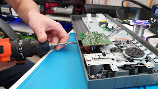
Now, drill a 6mm hole in the top of the +2 for the 3.5mm jack socket. I decided to place the jack socket in line with the power LED as this was close to where I was going to place the amplifier PCB.
I usually avoid any permanent ‘destructive’ modification but the other way of doing the mod involved some drastic PCB modification on the main board and loads of wires going from top to bottom of the +2 which would make any future mods awkward as I would have to remove the wiring to work on the +2. I also don’t like loads of excess wiring inside any console I modify.
The plastic housing is quite soft so take care not to push too hard on the drill... Let the drill bit do the work! On a safety note, it is advisable to wear safety glasses when drilling.
Next up, remove the white wire from the position highlighted below
I simply heated the solder joint and gently pulled the wire out from the underside of the PCB.
Now we need to prepare the 3.5mm jack socket before fitting by soldering the white and black wires to the relevant terminals.
Firstly, strip 12mm of insulation from the white wire then twist the wire strands together and tin.
Then place the wire through the Left and Right terminals of the 3.5mm jack socket then solder.
Now strip about 5mm insulation off of the black wire and fit it through the GND terminal of the jack socket. Note that I used my cutters to hold the wire in place when soldering.
Finally, cut some heatshrink sleeving and insulate the GND terminal.
Now fit the 3.5mm jack socket;
this can be quite fiddly! I found that my good long nosed pliers were narrow
enough to fit into the slots on the slotted nut of the jack socket which made
tightening the socket relatively easy.
Now strip twist and tin about 5mm on the remaining wires (Red, Yellow and Black)
Solder the Red wire in the position highlighted in the photo below
Then solder the black wire in the position highlighted below
Now solder the Yellow wire in the position highlighted below
And then tidy up the wiring using cable ties and an adhesive aluminium cable clip.
Remember to add the white wire from the PCB connector as well as the black and white wires from the 3.5mm jack socket into the wiring loom.
The PCB was made very narrow so that it would fit inside the +2 where I wanted it to go so I had to modify the adhesive based PCB Stand offs so that they would fit the PCB.
This was pretty straightforward, all I did was cut half of the plastic base off the stand offs (see picture below)
Now fit them to the PCB with the trimmed edges pointing towards the middle of the PCB. Note: I had to enlarge the holes of my PCB slightly to allow the standoffs to fit correctly. This was due to me making using Via’s instead of simple holes when designing the PCB. I am guessing that the plated through hole material narrowed the holes on the PCB.
Stick the PCB on to the +2. Note: it is very easy to place the adhesive pads on to the wires so care should be taken to ensure that the wires run freely through the middle of the underside of the PCB.
Now we have to wire the PCB up. Below is a simple wiring diagram.
Firstly, trim the wires to length.
Strip, twist and tin approx. 8mm of insulation off each end of the wires then fit as shown below.
Don’t forget about the white wire going to the PCB Connector!
Tidy up the wiring using the other adhesive aluminium cable clip.
And finally you should have something looking like this.
Now it is time to refit the +2 for testing.
Firstly, gently refit the keyboard membrane.
Then refit the PCB connector (this should only go in one way)
Now refit the six case screws.
Now it is time to test!
Set up your +2
Everything is hooked up; I am using my scart lead and have my TZX Duino plugged into the new 3.5mm jack socket. I have plugged in a dodgy old joystick which I am going to have to look at. Picture looking ok, now time to load a game.
Select Tape Loader on the +2 then play a file on the TZX Duino.
...
...
...
Hit play on the TZX Duino
And...
...
...
Looking and sounding very good; nice clear loading sounds coming from the +2
There was as always when loading any ZX Spectrum games an agonising wait... this time it was around five minutes!
But...
...
...
My patience was rewarded when it finally loaded
Success!!!
Time to relax with some Monty on the Run fun!
Below is a link to my Youtube clip of this whole process from start to finish.
Thank you for taking the time to read this rather long entry; I hope you found it useful and interesting.
All schematics, board layouts, gerber files and components listings can be found on my github should you wish to make a TZX amplifier circuit of your own.
https://github.com/Alleged-Geek/TZX-Duino-Amplifier-for-ZX-Spectrum-2
If you have any questions or comments please feel free to post a message either here, my Youtube channel, my Github site or email me at
I have a few other modifications I am planning for this computer and I am hoping that it won’t take as long to post about them as it took me for this entry.
Thanks again
Alleged Geek
- Get link
- X
- Other Apps
Popular Posts
ZX Spectrum +2 (grey) Cassette Drive Overhaul, Repair and Restoration
- Get link
- X
- Other Apps


Comments
Post a Comment