Repair and restoration of retro consoles, 8 bit computers. In this blog I hope to show you how to repair, retrore and modify old consoles and handhelds, from manufacturers such as Atari Amstrad Acorn Sinclair Commodore Dragon Sony MSX BBC Playstation Sega Microsoft xbox Spectrum ZX81 Vic 20 VIC20 C64 Amiga Binatone Grandstand.
Apologies for the delay with this entry; varied reasons include school holidays, two birthdays and some minor repairs of some retro console birthday gifts! Please feel free to use my PCB and 3D printed housing designs found on my Github and Thingiverse should you wish to make your own joystick adapter. Here is the TI994a working with the FlashRom99 and my Joystick Adapter circuit. Here are all the components required for this mod. The gerber files for my PCB design can be found on my Github. https://github.com/Alleged-Geek/TI99-4a-Joystick-Adapter/ And you are looking for the zip file named below if you are going to send the gerber file off to be manufactured. ti99-4a-adapter_2022-07-27.zip My github also contains stl files for printing the housing. And here is my version of the schematic diagram. You will need 10 X IN4148 signal diodes which can be found on eBay. 1 X DB9 D-SUB 9 Pin Female connector, again found on eBay. 2 X DB9 D-SUB 9 Pin Male connector al...
Get link
Facebook
X
Pinterest
Email
Other Apps
ZX81 Composite Video Mod and 16k internal Ram Upgrade + Re-Cap (part 2)
ZX81 Composite Video Mod and 16k internal Ram Upgrade +
Re-Cap (part 2)
Part 2: Installation of the Video Mod Circuit and 16k
Internal Ram (With a Re-Cap as an added bonus)
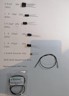
You will need the following components to do the memory
and Re-Cap Mod
1 x TC55257BPL-10L Memory Chip (I think I paid under £3
for it)
(there are several other suitable alternative memory
chips available)
1 X 22uF 16V (or greater) Radial Electrolytic Capacitor
1 X 1uF 16V (or greater) Radial Electrolytic Capacitor
Some thin equipment wire
In Part 1 I populated my video mod circuit.
Now we need to open up the ZX81.
Remove the three of the four rubber feet to reveal all
5 fixing screws.
Then remove the 5 fixing screws using a small crosshead
screwdriver and remove the bottom of the ZX81. You should be left with
something looking like this. Remove the two fixing screws which are highlighted
in the picture below.
After the screws have been removed, gently lift the PCB
up from the edge with the aluminium heatsink. Don’t overstress the keyboard
membrane as they are very easily broken. Just lift the PCB up enough until you
can get your fingers under and gently and very carefully pull the two membrane
connectors from their sockets.
Once removed, we need to de-solder the two wires from
the modulator.
The picture below shows the location of the modulator.
And the picture below shows a close up of the 2 wires
we need to remove before removing the actual modulator.
It is easier to de-solder from the solder side, so
below is a picture with the two solder joints highlighted.
Take care when de-soldering as 40 year old PCB’s can be
pretty fragile!
Now we need to de-solder the two fixing points for the
actual modulator itself. This is not an easy job and it took me several
attempts at de-soldering, followed by adding fresh solder until the modulator
was clear to come out.
I actually ended up using a prying tool whilst heating
the stubborn 0V pin which is used to secure the modulator to the PCB.
De-solder the two highlighted Via’s; you may want to
turn your soldering iron’s temperature up a wee bit if you can for this as it
takes a fair bit of heat to melt the solder. Don’t go too high with the
temperature though as you can easily damage the traces and via’s with very high
temperatures.
Despite my best efforts, I couldn’t clear the via’s of
solder so I added fresh solder and tried again.
Still no joy! Time for a different approach. This is a
wee cheat and I wouldn’t usually recommend it as you can easily damage the
traces and vias of the PCB whilst doing it.
If you are very careful, heat up one pin of the
modulator then whilst the heat is still on, use a prying tool to gently lift
the modulator up on the side you are heating.
After doing both sides, the modulator will fall off.
Clean up the vias by adding fresh solder to them then de-soldering each via
which should leave you a nice clean hole which will make the refitting a whole
lot easier.
As I was planning to do the memory mod as well I
decided to do all my de-soldering at this point so I removed the 1k memory
chip.
I couldn’t find my chip removal tool so I used my
prying tool to remove the chip. Care should be taken doing this as if you pry
the chip up too much on one side you could bend the legs of the chip. So the
best way to do this is to edge the chip up slightly on one side, then do the
same to the other and repeat until the chip is removed.
Once removed, de-solder the socket. This is quite
awkward and care should be taken not to damage the traces or via’s. Highlighted
below are the solder joints which need to be de-soldered.
All 28 via’s should be de-soldered (even the ones not
in use as the replacement memory chip is a 28 pin device)
De-soldering this was difficult as a few of the via’s
just wouldn’t de-solder. In the end I managed to remove the plastic housing of
the IC socket and picked off the rouge pins individually by using the heat and
pull technique used in the removal of the modulator.
I can’t stress highly enough about the care you need to
take doing this as the traces are very thin in some places.
Below is a picture of me heating the via and gently
removing the IC socket connectors.
After removing all the connectors, refill each via with
fresh solder then de-solder all 28 vias which should leave nice clean holes as
we did with the modulator.
After that, I would recommend cleaning all areas with
IPA and a cotton bud. That will remove any excess flux residue and it will give
you a nice and clean area to inspect for any damage after the trauma caused by
thede-soldering process.
Look at the state of that cotton bud!
Place the new 28
pin IC socket into the circuit. Care should be taken to put the IC socket in
the correct way round. The photo below highlights the end that the notch on the
socket should be situated.
Then solder the opposite corners of the IC socket,
check that the socket is sitting flat against the component side of the PCB
then if so, solder the remaining via’s.
Now let’s revisit that modulator; we need to strip
everything out of it! This is another awkward process, the 5 solder points
which secure the modulator PCB to the housing needs quite a bit of heat to
remove. I have highlighted the solder points in the picture below.
After a bit of huffing and puffing, you should end up
with something looking like this.
Time to fit the new circuit board.
This is quite a fiddly process but I will try and
explain the best I can with photos taken from a video clip.
The White and Red wires are fed through the two holes
in the plastic bush. The White wire is a bit of a struggle as I used 7/0.2mm
equipment wire. I actually had to strip some insulation off the end of the
white wire, tin it then feed it through the smaller of the two holes. Once the
stripped wire was through I managed to pull the white wire through. It is made
more awkward due to the RF (now composite) socket.
The Red wire easily fits through the larger of the two
holes.
With the Red and White wires fitted, it is now time to
fit the video mod PCB into the modulator housing. The easiest way to fit it is
to put it in at an angle from the bottom of the modulator housing, then it
should just snap into place.
Apologies for the above photo where you can hopefully
see that the board is sitting nicely in the modulator housing. Once fitted it
is time to wire up the Yellow and Black wires.
I started with the Yellow wire; it goes to the middle
terminal of the old RF socket.
Measure the wire and cut to length.
Then strip, twist and tin the end of the yellow wire
and solder it on to the centre pin.
Now measure the length and cut the black wire to size.
And strip, twist and tin the end of the wire then
solder the wire on to the corner directly opposite the yellow wire (there
should already be solder on a part of the modulator housing so it should be
relatively straightforward.
Now fit the bottom lid of the modulator remembering to
replace the original brown/red insulator.
Now fit the top lid
Here is where we want to fit the Red and White wires,
the modulator covers the text which makes things a wee bit more awkward but it
should be the only two empty of solder Via’s.
Now fit but do not solder the modulator as this will
make things easier to solder.
Measure the Red wire, cut to length, strip, twist and
tin the end.
Pop the bare wire through the correct Via, then solder.
Now measure the white wire, cut to length, strip, twist
and tin the end.
And for soldering this wire, I found it easier to
remove the modulator from the PCB, pop the stripped white wire through the
correct Via then solder.
Refit the modulator then solder the two pins; this may
take a wee bit of heat from the soldering iron as the legs of the modulator are
pretty thick.
Job Done!
Now we are going to fit the 16k memory chip!
After some
research, I picked up a TC55257BPL-10L SILICON GATE CMOS STATIC RAM from Ebay
for a couple of pounds and decided that I would try to modify my ‘fun’ ZX81 so
that it had internal 16K Ram instead of the very unreliable ram pack which I
have for it. Like all ZX81 owners know, the ram pack wobble is the most
frustrating thing in the world!
Before we start this mod, we need to change the wired
link 1 to link 2 on the right hand side of the ram chip. I have highlighted
Link 1 with a pin on the picture below.
Below is a picture of the Via’s which need to be
de-soldered
Once de-soldered, remove the link and place it in the
L2 position. Alternatively, if you lost the link (as I did) simply use a
resistor leg to make a new one.
Then solder the link.
Once that is done we can move on to the main part of
this mod.
The mod itself didn’t look too intimidating (although
de-soldering the original 1k ram wasn’t fun… well it was really ;o)) all I had
to do was bend a few pins out then solder them to some of the diodes beside the
keyboard membrane.
Here is a picture of the TC55257BPL-10L I purchased.
From what I had read, I would need to bend out pins 1,
21, 23 and 26 as they would need to be connected topins 1, 40, 2 and 3 of the Z80 chip
respectively.
Fit the 28 pin device into the ZX81; note that the
notch on the chip matches the notch on the socket
I trimmed down the four unconnected pins of the IC.
Then I tinned (added solder) to the pins which would
make soldering the wires on to them a whole lot easier.
Now I am going to add solder to the Diodes I am going
to be connecting via wires.
They are in order as follows
Starting with D1
Now D2
Next up D3
And
finally D5
Now it is time to wire them up. I will admit here that
I did this mod yesterday and it worked first time. However I was not happy with
the wiring! I put everything back together and slept on it. When I woke up this
morning, I decided that I was going to change the wiring as although it worked,
it was a bloody mess in my opinion! A hidden mess but it didn’t sit well with
me.
Below is a picture of the messy wiring job I did yesterday!
I thought that I could get away with using my preferred
7/0.2mm equipment wire but it looks a mess… a functional mess I grant you but
still a mess!
So this morning after a restless sleep I opened up the
ZX81 again, removed the old wiring then set about re-soldering the wires.
I could have used some 10/0.1mm equipment wire which
looks ok and is a much more flexible than the 7/0.2 but in the end I decided to
use some Kynar wire (or wire wrap wire as I know it… showing my age here ;o))
Firstly we need to strip and tin the end of the Kynar
wire. I wish I still had my wire wrapping tool which had a stripping function
on it! This is quite fiddly as if you try removing the insulation with your
cutters it is very easy to cut through the wire completely.
What I ended up doing in most cases was to use my
soldering iron to melt the insulation at about 5mm then pick it off with my
fingernails.
Below is a picture of me tinning the end of the Kynar
wire
Now solder that to Pin 1 of the memory IC.
Measure the length of wire and cut to size.
Then strip and tin the end of the wire.
Finally, solder the wire on to D1.
And
hopefully you will have something looking like this.
Now we are going to connect Pin 21 of the IC to D2
using exactly the same process as above.
Next up is Pin 23 of the IC to D3.
And finally Pin 26 of the IC to D5.
Job done! Memory upgrade complete!
I could have stopped there but decided that as I was
inside my ZX81 anyway, it would be a good time to Re-Cap it as well.
There are only two capacitors that we really need to be
concerned about and they are
C3 which is a radial 22uF Electrolytic Capacitor
And
C5 which is another radial Capacitor but is only 1uF
Capacitors of this age can sometimes dry out and cause
damage to your circuit. You can usually spot any signs of failing capacitors by
examining the casing of the capacitor; look for bulging at the top, any signs
of leakage at the base of the capacitor on the component side and finally look
at the solder joints for any kind of residue.
Luckily for me both capacitors looked good but as they
are now 40 years old I decided to replace them anyway.
Below is a picture of the location of C3.
This is a 22uF 16V capacitor; the replacement I had was
a 22uF 63V. It doesn’t matter if the voltage rating is higher so the 63V
capacitor will work absolutely fine but it is always a bad idea to select a
lower voltage rated capacitor as these will get hot and more than likely leak,
then dry out.
Below is a picture of my replacement capacitor.
Let’s have a look for the Via’s so that we can de-solder
C3.
De-solder the two Via’s next to the pin and remove C3.
Then Fit the new capacitor.
Care should be taken at this point as placing C3 in the
wrong way round will cause the capacitor to fail and in some circumstances
explode. I actually show this to my students as a demonstration that some components
must be fitted correctly… it usually does the trick ;o)
Let’s take a closer look at C3
The tweezers are pointing to the positive leg of the
capacitor (which is almost always longer than the negative leg when the
capacitor is new) if you follow the short leg up to the capacitor, you will
notice that there is a grey/blue stripe with negative signs printed along it.
Highlighted below is the positive via on the PCB.
Fit the new C3 into position as shown below then
solder.
Now let’s find C5 on the component side of the PCB.
The via’s we need to de-solder are highlighted by the
pin in the picture below.
De-solder both Via’s then remove C5.
Below is a picture of C5 with the positive leg
highlighted with the pin.
Below is a picture of where the positive leg goes on
the circuit board.
Fit the new 1uF C5 then solder.
And that is all the modifications complete!
Now we have to put everything back together and test…
nervous times!!!
Before we refit the keyboard membrane, remember to refit
the dust shield.
Carefully refit the keyboard membrane.
Then refit the two smaller silver fixing screws.
Refit the bottom cover using the 5 longer black screws.
And finally refit the rubber feet. You may need to
clean the old glue off the feet and computer base beforehand then use double
sided tape to re-stick the feet.
Set the ZX81 up as shown; remember to use the composite
input!
Plug it in.
And.
…
…
…
Success!!! We have the K! great start!
Now to test the upgraded internal memory.
Type the following code into your system; I have to
admit that it took me quite a while to remember how to use the functions!
Then run the program.
There was an agonising wait!
…
…
Then this happened!
Success!!! Good job!
Now to test it with a game; I chose Scramble this time.
Load “”
There was another agonising wait for about a minute and
a half as my screen went blank (due to my telly not recognising the noisy
signal from the ZX81)
But then this happened.
Success!!!
I decided to have a bit of fun with this game and
played it for about an hour without the dreaded Ram Pack Wobble interfering
with play!
Great fun was had!
Well, that is another entry all but over. Please find
below a youtube video of me doing most of the work written about above.
This was a truly amazing wee project to work on. It
started when I wanted to try my new PCB layout which was printed by JLPCB.
Not content with just that and as this was my spare
zx81, I wanted to try something different. The memory mod was fantastic! It was
quite difficult getting reliable information about this project as there was
little in the way about modifying an issue 1 ZX81 (plenty about the Issue 3
though)
I also took a bit of a gamble with the CMOS Ram chip; it
wasn’t one I had seen used by anyone but it had the same functions and a
similar pin out so I gave it a go.
The Re-Cap was just an afterthought and I am glad I did
it!
I hope that this entry has been interesting for you; I
am not an expert by any means but if you have any questions or queries about
the above modifications then please feel free to get in touch either though
this blog or email.


Comments
Post a Comment